1. Positive Clipper
The clipper which removes the positive half cycles of the input voltage is called the positive clipper. The circuit arrangements for a positive clipper are illustrated in the figure given below.
- Positive Series Clipper and Positive Shunt Clipper
The figure illustrates the positive series clipper circuit (that is, diode in series with the load). From the figure (a) it is seen that while the input is posi tive, diode D is reverse biased and so the out put remains at zero that is, positive half cycle is clipped off. Dur ing the negative half cycle of the input, the diode is forward biased and so the nega tive half cycle appears across the output.
Figure (b) illustrates the positive shunt clipper circuit (that is, diode in parallel with the load). From the figure (b) it is seen that while input side is positive, the diode D is forward biased and conducts heavily (that is, diode acts as a closed switch). So the voltage drop across the diode or across the load resistance RL is zero. Thus output voltage during the positive half cycles is zero, as shown in the output waveform. During the negative half cycles of the input signal voltage, the diode D is reverse biased and behaves as an open switch. Consequently the entire input voltage appears across the diode or across the load resistance RL if R is much smaller than RL
Actually the circuit behaves as a voltage divider with an output voltage of [RL / R+ RL] Vmax = -Vmax when RL >> R
Note: If the diode in figures (a) and (b) is reconnected with reversed polarity, the cir cuits will become for a negative series clipper and negative shunt clipper respec tively. The negative series and nega tive shunt clip pers are shown in figures (a) and (b) as given below.
- Negative Series Clipper and Negative Shunt Clipper
In the above discussion, the diode is considered to be ideal one. If second approximation for diode is considered the barrier potential (0.7 V for silicon and 0.3 V for Germanium) of diode, will be taken into account. Then the output wave forms for positive and negative clippers will be of the shape shown in the figure below.
- Output Waveform – Positive Clipper and Negative Clipper
2.Biased Clipper
Sometimes it is desired to remove a small portion of positive or negative half cycles of the signal voltage. Biased clippers are employed for this purpose. The circuit diagram for a biased negative clipper (that is for removing a small portion of each negative half cycle) is illustrated in figure (a).
- Biased Negative Clipper
The action of the circuit is explained below. When the input signal voltage is positive, the diode D is reverse-biased and behaves as an open-switch, the entire positive half cycle appears across the load, as illustrated by output wave form [figure (a)]. When the input signal volt age is negative but does not exceed battery voltage V, the di ode D remains reverse-biased and most of the input voltage ap pears across the output. When during the nega tive half cycle of input signal, the signal voltage exceeds the battery voltage V, the diode D is forward biased i.e conducts heavily. The output voltage is equal to – V and stays at – V as long as the input signal voltage is greater than battery voltage V in magnitude. Thus a biased negative clipper removes input voltage when the input signal voltage exceeds the battery voltage. Clipping can be changed by reversing the battery and diode connections, as illustrated in figure (b).
- Biased Positive Clipper
Some of other biased clipper circuits are given below in the figure. While drawing the wave-shape of the output basic principle discussed above are followed. The diode has been considered as an ideal one.
- Biased Clipper Circuits
- Different Clipping Circuits
3. Combination Clipper
When a portion of both positive and negative of each half cycle of the input voltage is to be clipped (or removed), combination clipper is employed. The circuit for such a clipper is given in the figure below.
Combination Clipper
The action of the circuit is summarized below. For positive input voltage signal when input voltage exceeds battery voltage + V1 diode D1 conducts heavily while diode D2 is reversed biased and so voltage + V1 appears across the output. This output voltage + V1 stays as long as. the input signal voltage exceeds + V1. On the other hand for the negative input voltage signal, the diode D1 remains reverse biased and diode D2 conducts heavily only when input voltage exceeds battery voltage V2 in magnitude. Thus during the negative half cycle the output stays at – V2 so long as the input signal voltage is greater than -V2.
Read more: http://www.circuitstoday.com/category/clipping-and-clamping-circuits/page/2#ixzz0vtyytM5H
To summarize, a variety of series and parallel clippers with the resulting output for the sinusoidal input are provided below:
Figure 1: Shows the input
Figure 2: positive cycle clipped.
Figure 3: Negative cycle clipped.
Figure 4: Both the positive and negatice cycles are clipped.
Source: Study Electronics
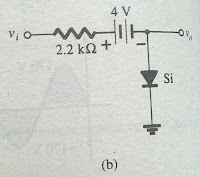
To further understand clipping circuits, here are the solutions to some problems in Electronic Devices and Circuit Theory (10th edition) by Boylestad and Nashelsky:
Problem 33 page 127
Determine Vo for each network for the input shown.

Problem 35 page 128


0 people rectified:
Post a Comment